undefined
Similar Products


Description
Multilayer PCBs represent the advanced solution for complex electronic systems, combining multiple conductive layers into a single, compact board. Manufactured by Renuka Electronic...
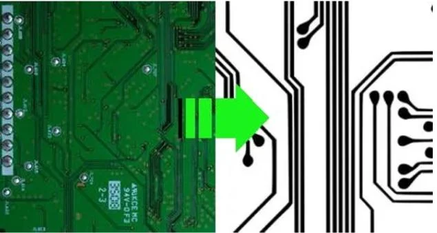
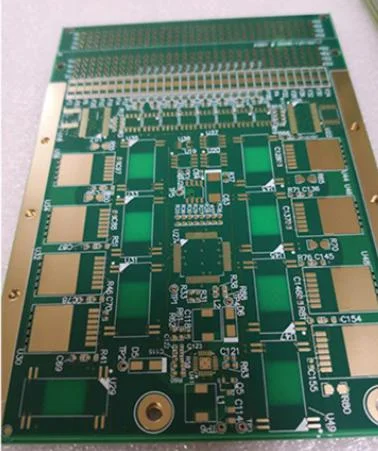
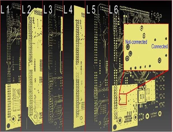
Multilayer PCBs represent the advanced solution for complex electronic systems, combining multiple conductive layers into a single, compact board. Manufactured by Renuka Electronics, these circuit boards are engineered to handle sophisticated circuitry while maintaining signal integrity and thermal management. The precise lamination process ensures each layer aligns perfectly, creating reliable interconnections that support high-density component placement. This construction method allows for more complex designs than traditional single or double-layer boards, making them essential for modern technology applications where performance cannot be compromised.

Across various industries, multilayer PCBs serve as the foundation for critical electronic systems. In telecommunications, they enable high-speed data transmission with minimal signal loss. Medical equipment manufacturers rely on their stability for diagnostic devices and monitoring systems. Industrial automation utilizes these boards for control systems that operate continuously in demanding environments. The automotive sector incorporates them into advanced safety features and vehicle management systems, while aerospace applications benefit from their lightweight yet durable construction for navigation and communication equipment.

The business value of multilayer PCBs lies in their reliability and suitability for demanding applications. Renuka Electronics ensures consistent quality through rigorous testing and precise manufacturing processes. These boards offer long-term performance stability, reducing maintenance needs and downtime in critical systems. Their robust construction withstands environmental challenges while maintaining electrical performance, providing peace of mind for engineers and system designers. The investment in quality multilayer PCBs translates to reduced failure rates and enhanced product longevity across all applications.

Key Features:
- Multiple conductive layers laminated together for complex circuit designs.
- Precise layer alignment ensuring reliable interconnections between circuits.
- High-density component placement capability within compact board dimensions.
- Enhanced signal integrity through controlled impedance and reduced crosstalk.
- Robust construction suitable for demanding environmental conditions.

Benefits:
- Supports sophisticated electronic systems with reliable performance under various conditions.
- Enables compact device designs through efficient use of available space.
- Reduces electromagnetic interference for cleaner signal transmission.
- Provides stable platforms for sensitive components requiring precise operation.
- Offers long-term durability with consistent electrical characteristics over time.
Specifications
| Additional Information | |
|---|---|
| Country of Origin | India |
| Customisable | No |
Application
Multilayer PCBs are essential for modern electronic systems where space constraints and signal integrity are paramount. Their layered construction allows for complex routing and high component density, making them ideal for sophisticated devices that require reliable performance under demanding conditions.

These circuit boards support high-speed data transmission and minimize electromagnetic interference through careful design. They accommodate advanced technologies by providing stable platforms for sensitive components, ensuring consistent operation across various environmental factors and usage scenarios.

Real-world applications:
- Telecommunications equipment requiring high-frequency signal processing and minimal interference.
- Medical devices where reliability and precision are critical for patient safety and accurate readings.
- Industrial automation systems that demand durable circuit boards for continuous operation in harsh environments.
- Automotive electronics for advanced driver assistance systems and vehicle control units.
- Aerospace and defense applications needing lightweight, high-performance boards for navigation and communication systems.
Trade Details
| Available Stock | In stock |
| Sample Availability | No |
Payment Terms
| Payment Terms |
|
| Payment Methods |
|
Company Profile

RENUKA ELECTRONICS, Karnataka Karnataka, India
Electronics & Electrical•Manufacturer
Factory Details
Factory SizeBelow 1000 sqm
Multilayer PCB for advanced electronic systems
Multilayer PCB from Renuka Electronics delivers high-density, reliable circuit boards for advanced electronics, featuring precise layer alignment and robust construction for performance-critical applications.
Min. Order Quantity: 1 pieces
Shipping
Shipping fee and delivery date to be negotiated. Contact supplier now for more details.
RENUKA ELECTRONICS
 Karnataka, India
Electronics & ElectricalManufacturer